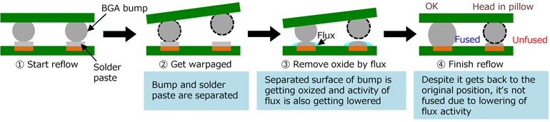
Head-in-Pillow (HIP) is a critical solder joint defect that occurs in printed circuit boards when the solder ball of a Ball Grid Array (BGA) and the corresponding solder paste deposit on the PCB fail to coalesce during reflow.
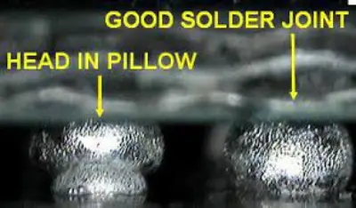
Visually, it appears as the BGA sphere resting on a pillow of solder, hence the name. Electrically, a HIP joint may initially pass tests (partial contact can conduct) but it has very weak mechanical integrity. Even minor thermal or mechanical stress can cause these joints to fail in the field.
IPC standards treat HIP as a critical defect. IPC-7095 defines it as: “a solder joint comprised of two metallurgically distinct masses… with incomplete or no coalescence”, and IPC-A-610 acceptability criteria mandate no evidence of head-on-pillow on any BGA joint.
While HIP is often attributed to warpage during reflow or flux issues, PCB design plays a surprisingly significant role in its occurrence. Design choices that influence solder wetting, pad co-planarity, thermal balance, and oxide prevention can all determine whether a BGA joint succeeds or silently fails.
In this article, we’ll explore four key design factors that impact HIP risk:
For each, we’ll examine how the design choice contributes to HIP defects and offer targeted troubleshooting and prevention strategies, referencing IPC standards and real-world best practices.
The geometry and layout of BGA pads directly affect solder joint quality, and poor pad design is a leading contributor to head-in-pillow defects.
One of the most critical choices is whether to use Non-Solder Mask Defined (NSMD) or Solder Mask Defined (SMD) pads:
Industry standards like IPC-7095 favour NSMD pads for BGA reliability. NSMD pads allow the solder to wrap around the pad edges, yielding a larger wetting surface and a taller post-reflow solder fillet (ball stands slightly higher). In contrast, SMD pads constrain the solder flow and effectively present a larger copper land that causes the ball to spread wider and flatter.
The larger pad area in SMD leads to a lower solder joint “crest height” after reflow. If the component or board warps, a flattened joint may not bridge any gap, resulting in an open (HIP) condition. To minimise HIP risk, designers should favour NSMD BGA pads of proper diameter (typically about 20% smaller than the ball) so that the solder ball retains a robust spherical fillet that can tolerate slight separation during reflow.
Vias placed directly in pads can siphon solder paste away during reflow, especially if left unfilled, leaving insufficient solder to contact the ball. This commonly results in HIP failures. To avoid this, use filled and capped vias or fan out via connections away from the pad.
IPC-7095 and IPC-7351 guidelines advise either avoiding vias in BGA pads or using filled/plated-over vias to ensure a flat, non-porous pad surface. Regardless of layout, pad planarity is crucial. Any dimples, damage, or debris on the pad surface can prevent proper solder wetting.
Troubleshooting tip: If HIP failures are clustered around specific BGA pins—particularly those connected to vias or sized differently—review the pad design closely. Increasing the stencil aperture (to deposit more paste), switching from SMD to NSMD, or redesigning the pad-to-via structure may resolve the issue.
The surface finish on a PCB pad directly affects solderability and plays a major role in head-in-pillow defects. A poor or oxidised finish can prevent proper fusion between solder ball and pad, even if both melt during reflow. Conversely, an ideal finish provides a solderable, oxide-free surface for the paste and ball to fuse.
Popular finishes like ENIG (Electroless Nickel/Immersion Gold) offer good planarity and shelf life, but they come with risks. Improper plating can cause the notorious “black pad” issue—where a brittle, oxidised nickel layer blocks solder bonding beneath the gold.
Other finishes also have solderability concerns:
Mechanism-wise, any surface oxidation or contamination can cause the solder ball to not wet the pad, leading to incomplete coalescence. During reflow, the solder ball may melt and even deform, but if the pad’s surface finish does not readily alloy with the solder (due to oxides or poor flux activity), the ball and paste remain separate.
To reduce HIP risk, always choose a surface finish that meets IPC J-STD-003 solderability standards and ensure it’s properly handled throughout manufacturing.
With ENIG, that means working with your PCB supplier to prevent black pad through controlled nickel plating. For OSP, limit storage time and, where possible, use inert reflow conditions to minimise oxidation. If HIP defects show signs of non-wetting like dull or grainy pad surfaces, the finish may be the root cause.
In such cases, switching to a more solder-wettable option or refreshing the existing finish can resolve the issue. Ultimately, finish quality and compatibility are critical; well-wetted pads are your first defence against head-in-pillow.
Troubleshooting tip: If HIP failures show dull, grainy pad surfaces or occur after prolonged storage, the surface finish may be to blame. Switching to a more solder-wettable finish—or requalifying your current one—can often resolve the issue.
Solder mask design influences how solder flows and solidifies during reflow—especially under BGAs. One key factor is whether the pad is solder mask defined (SMD) or non-solder mask defined (NSMD).
NSMD pads allow solder to wet both the top and sides of the pad. This produces a taller, more resilient joint. In contrast, SMD pads restrict solder to the top surface, creating flatter joints that are more vulnerable to HIP if separation occurs during reflow. IPC-7095 and 7351 both recommend NSMD pads for BGA reliability. In one reported analysis, HIP defects were mostly eliminated by switching from SMD to NSMD pad design, confirming the importance of mask-defined pad geometry.
Beyond pad definition, the solder mask layout around each pad plays a crucial role in joint formation. If the mask encroaches on the pad—due to poor registration or insufficient clearance—it can block part of the copper surface, reducing the area available for solder to bond. This partial coverage may prevent full wetting, especially on one side of the ball. To avoid this, designers should allow for sufficient mask expansion—typically about 0.1 mm larger than the pad diameter for NSMD pads—to ensure a clear gap around the copper land.
Where space allows, solder mask between adjacent pads (known as webbing) should also be retained. While primarily used to prevent solder bridging, it helps keep paste in place during reflow. If this mask web is too narrow or missing entirely, paste may slump or shift, potentially disrupting how the ball and pad merge. For HIP specifically, the key concern is not bridging, but incomplete pad exposure—often caused by poor mask alignment or overspill.
Troubleshooting tip: Inspect boards for solder mask misregistration or solder mask residues on pad surfaces if sporadic HIP defects occur. During process validation, verify that the mask-defined pad sizes match design intent. The best practice is to use NSMD pads with well-aligned mask openings, so each BGA land is fully exposed and evenly wetted.
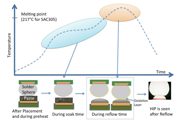
How traces and copper planes connect to BGA pads can significantly affect solder joint quality, especially during reflow. One common issue is uneven thermal distribution. If a BGA pad is directly tied to a large copper pour, like a ground or power plane, it may heat more slowly than isolated pads. As a result, the solder ball may melt and oxidise before the pad’s solder paste reaches liquidus, leading to poor wetting, or a head-in-pillow joint.
To mitigate this, designers should balance the thermal mass on all BGA pads. Pads connected to planes should include thermal reliefs—thin spokes or narrowed traces—to slow heat transfer and allow even reflow. IPC-7095 recommends avoiding large direct copper connections and instead using dog-bone fanouts or via-in-land only when filled and capped.
Trace routing geometry can also affect solder joint shape. If a trace to a BGA pad enters off-centre, it can create an asymmetric solder distribution. In extreme cases, more solder may wet along the trace side of the pad, and less on the opposite side, which could leave a portion of the ball not fully wetted. A mitigation strategy is to use teardrop pad connections—tapering the trace as it meets the pad in a rounded fashion.
This not only strengthens the pad mechanically (reducing risk of pad cratering or trace cracking) but also provides a more uniform pad shape for soldering. Teardrops ensure the solder sees a gradual transition and the pad remains essentially round, promoting even wetting. Additionally, avoid any abrupt changes in copper thickness near the pad.
For instance, if heavy copper is used on internal layers, ensure the BGA pads have consistent copper thickness and aren’t adjacent to large copper features that cause localised cooling. From a design for manufacturability (DFM) standpoint, it’s wise to keep all BGA pads as consistent as possible – same size, same copper connection style, and all vias either in pad (and filled) or equally offset in a dog-bone fanout. This consistency helps solder joints form uniformly.
Troubleshooting tip: If the defect correlates with certain nets (like all power pins), consider the layout; reducing copper on those pins or adding thermal isolation can help correct the issue.
Preventing HIP defects requires a holistic approach, marrying good PCB design practices with controlled assembly processes. On the design side, we have seen that proper pad design, finish selection, mask definition, and routing can each eliminate potential root causes of head-in-pillow.
Following IPC-7095 guidelines for BGA implementation is highly recommended. This includes using adequate NSMD pad sizes, filling or tenting vias, and selecting high-solderability finishes.
During design reviews, explicitly check for features that might induce HIP:
Many CAD tools offer DFM rules to flag such items (for example, flagging any unfilled via in a BGA pad or insufficient mask clearance). Incorporating those checks in the PCB design validation can catch HIP-prone features before boards are fabricated.
On the manufacturing side, even with a robust design, process parameters should be optimised to further mitigate HIP. This includes using a solder paste with good flux activity/life, ensuring accurate part placement (proper pressure to seat balls into paste), and dialing in the reflow profile (adequate soak to minimise warpage, not overheating the flux). However, if a HIP issue persists, a feedback loop with design is essential.
For instance, X-ray inspection results may reveal a pattern to the opens, pointing back to a design tweak as the fix rather than just process tweaks. Remember that HIP defects often manifest at the edges or corners of BGAs (areas most susceptible to warpage), so paying special attention to design symmetry and support in those regions can help. IPC-A-610 classifies a non-coalesced BGA joint as a defect (non-wet open), so any occurrence in production is cause for corrective action.
By applying the strategies discussed, correct pad and mask design, high-quality finishes, and balanced trace layout, PCB designers can greatly reduce the incidence of head-in-pillow at the source. In tandem with assembly best practices, these design measures ensure robust BGA solder joints that meet IPC-610 criteria for full wetting and reliability. The end result is a manufacturing process more forgiving to variation, and BGA connections that perform reliably in the field without the hidden risk of “head-in-pillow” failures.
J-TEQ is fully aligned with multiple international standards and our highly trained technicians carry the expertise to both build PCBs to meet said standards and identify and correct problems when they occur. Speak to us today about your projects.