Via-in-Pad, Plated Over (often referred to by the acronym VIPPO), and epoxy-filled microvias are two advanced via technologies often used in tandem in high-density PCB designs. These are often used for complex devices such as those found in smartphones, medical devices, or aerospace systems.
When designing a printed circuit board for manufacturability, it is vital we choose technologies that best support the functionality of the device and the practicalities demanded by production lines. Let's take a closer look at each of these technologies and how they work, plus their pros and cons and how they should be used.
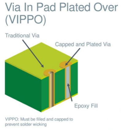
VIPPO refers to a process where a via (typically a through-hole or blind via) is drilled directly in a component pad, filled with conductive or non-conductive material, and then plated over and finished to create a flat, solderable surface.
They are created using the following method:
Choosing VIPPO brings several benefits. Firstly, it offers a space-saving solution for high-density layouts. For complex PCBs that require many electronic components in a finite amount of space, VIPPO offers flexibility. BGA, QFN, and CSP arrays can all benefit from the VIPPO layout.
The short interconnected path also provides improved thermal and electrical performance, and the planar surface offers better solder joint integrity than other design options.
Using VIPPO does present a few risks and challenges, particularly around high manufacturing complexity and costs. Finding a certified expert EMS such as J-TEQ will be a must.
There are also several manufacturing risks that need to be mitigated. VIPPO requires precise planarity for good soldering. They are susceptible to the risk of voids or incomplete fills, which could affect their reliability. If done incorrectly, it could cause pad cratering or delamination during reworking processes.
The best practices to follow are found in the IPC-4761 Type VII guidelines. Cap plating thickness should be kept at more than 25 μm for proper planarity. VIPPO details should be kept in all Gerber and fabrication drawings. Using VIPPO in high-thermal stress areas should be avoided unless qualified to do so.
Microvias are laser-drilled holes (typically less than 150 µm in diameter) used to interconnect layers in HDI boards. They have a conductive epoxy filling to strengthen the structure and allow stacking or capping with copper for component mounting.
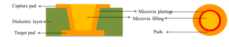
These microvias are created using this method:
Epoxy-filled vias are a good choice for HDI (High-Density Interconnect) designs. They have better signal integrity, as they offer shorter paths with lower inductance, and they allow stacked vias for multi-layer routing.
However, there is a risk of cracking under thermal cycling due to a CTE mismatch, and stacking more than two can prove to be unreliable. There is a risk of resin smear and an incomplete fill, and it can prove to be a costly process due to the need for laser drilling and other material requirements.
Best practices are dictated by IPC-2226 for HDI design rules. Staggered microvias are often preferred over stacked ones. The epoxy resin should be chosen carefully to ensure its CTE matches with the base laminate. During the filling process, the vias should be carefully checked to ensure a full fill and a good copper cap for reliable connections.
So, in summary:
| Feature | VIPPO | Epoxy-Filled Microvias |
| Drilling | Mechanical | Laser |
| Fill Type | Epoxy or conductive + copper cap | Epoxy fill + optional copper cap |
| Pad Integration | Directly in component pad | May terminate under or away from pad |
| Use Case | Fine-pitch BGA/GFN, RF | HDI, mobile, aerospace, stacked vias |
| Manufacturing Cost | High | High |
| Reliability (Thermal) | Moderate (planarity/pad risk) | Moderate-High (CTE mismatch risk) |
DFM awareness allows us to consider the practical risk of processes like VIPPO and epoxy-filled microvias, highlighting practical risks and avoiding production issues in the future. Common risks and recommended actions for these processes include:
| Process Step | Common Risk | DFM Guideline/Threshold | Recommended Action |
| Electroless Copper Plating | Poor adhesion to epoxy, internal stress, voids | Needs well-prepared, polar resin surface | Use only with resins proven compatible with process |
| Direct Metallisation | Surface variability, graphite overexposure | Apply uniform graphite coating with optimised fixer | Recommended for smooth, non-polar, epoxy plug surfaces |
| Vacuum Epoxy Fill | Voids due to trapped air | Use vacuum-assisted fill with CTE-matched epoxy | Specify void-free fill requirement in fab notes |
| Epoxy Cure | Shrinkage leading to dimples | Dimple depth >25 µm may cause solder voids | Identify pads with >25 µm recess for review |
| Surface Grinding | Over-grind exposing copper or undercut | Maintain flatness within ±10µm across pad | Include max grind depth spec in fab drawing |
| Copper Cap Plating | Thin plating over epoxy | IPC Class 3: ≥25µm average, ≥20 µm minimum | Target ≥25 µm copper cap thickness |
| Flying Probe Test | Pad damage, ENIG fracture, voiding | Avoid Flying probe VIPPO pads with ENIG finish | Route test access to non-VIPPO pads |
| ENIG Finish | Brittle nickel layer prone to cracking | Avoid mechanical stress post-ENIG | Use AOI/X-ray instead of probe test |
One key area of DFM to be aware of is the importance of choosing the correct epoxy for the project. Though copper or other thermally conductive filling may be appropriate for some, others may benefit from a non-conductive material filling such as a standard epoxy resin.
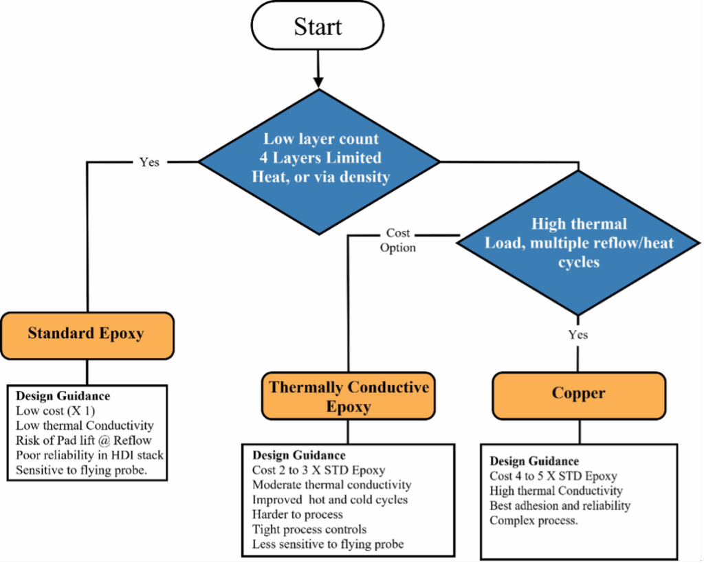
The via filling should be applied in a vacuum to enhance the wetting of the via walls and copper plating and to help get rid of trapped bubbles. During the various reflow stages, each epoxy faces the following risks and outcomes:
| Reflow Stage | Standard Epoxy | Thermal Epoxy | Copper Fill |
| Preheat | Risk of CTE mismatch Pad lift if ramp rate too aggressive<3°C Ramp | Better thermal match filler separation possible if ramp is too high | Excellent thermal match Stable under controlled ramp |
| Soak | Resin softening begins Voiding risk if epoxy not fully cured (More likely in second reflow) | Filler dispersion critical Resin-rich zones may form | Minimal change Stable grain structure |
| Reflow Peak | High stress on pad/via interface Delamination possible; flying probe indent pose a voiding risk (More likely in second reflow) | Filler integrity tested Risk of thermal gradient stress Minimise peak reflow and TAL | Solid fill resists deformation Risk only if plating is thin or uneven |
| Cooling | 2 to 3°C/sec cooling rate Minimise shrinkage stress; avoid pad lift or delamination | Controlled cooling needed to avoid filler separation | Low risk; solid copper contracts uniformly |
In complex, space-constrained PCB designs, VIPPO and epoxy-filled microvias each bring unique strengths and are often used in combination to meet both electrical and structural demands. By adhering to DFM best practices and industry standards, designers and manufacturers can minimise risk and optimise reliability.
Partnering with a trusted EMS like J-TEQ ensures your PCB is built right, from layout to final inspection. Our team can guide your design through material selection, process control, and compliance. Get in touch today to find out more.