Introduction
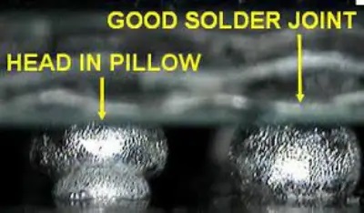
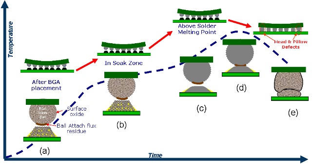
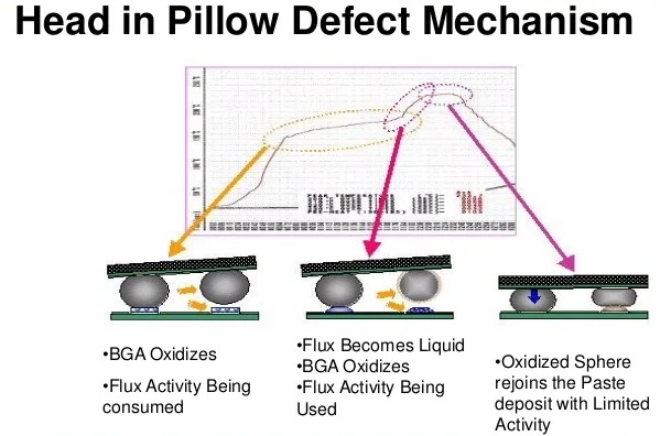
Head-in-Pillow (HIP) is a solder joint defect where a BGA solder ball and the PCB solder paste deposit do not fully merge, resulting in two separate, non-coalesced solder masses. Visually, it appears as the BGA sphere resting on a pillow of solder – hence the name. Electrically, a HIP joint may initially pass tests (partial contact can conduct) but it has very weak mechanical integrity. Even minor thermal or mechanical stress can cause these joints to fail in the field. IPC standards treat HIP as a critical defect: IPC-7095 defines it as “a solder joint comprised of two metallurgically distinct masses… with incomplete or no coalescence”, and IPC-A-610 acceptability criteria mandate no evidence of head-on-pillow on any BGA joint. While HIP often stems from component or PCB warpage during reflow and insufficient flux activity, PCB design choices can greatly influence HIP occurrence. In this article, we focus on four design factors – pad design, surface finish, solder mask design, and track layout – and explain how each can contribute to HIP defects during reflow. We also highlight troubleshooting and prevention strategies, referencing IPC-610/7095 best practices that manufacturing engineers and PCB designers can apply.
Pad Design and HIP Risk
Pad geometry and layout play a pivotal role in BGA solder joint formation. If a pad is improperly sized or configured, it may prevent the solder ball from wetting completely. One key design choice is using Non-Solder Mask Defined (NSMD) vs. Solder Mask Defined (SMD) pads. NSMD pads expose the full copper land, whereas SMD pads have the solder mask overlap the pad edges (reducing the exposed area). Industry guidance (including IPC-7095) generally recommends NSMD pads for BGA lands to improve wetting and reliability. NSMD pads allow the solder to wrap around the pad edges, yielding a larger wetting surface and a taller post-reflow solder fillet (ball stands slightly higher). In contrast, SMD pads constrain the solder flow and effectively present a larger copper land that causes the ball to spread wider and flatter. Studies have shown that head-in-pillow defects are far more prevalent (up to ~87% higher) with SMD pad designs than with NSMD. The larger pad area in SMD leads to a lower solder joint “crest height” after reflow – if the component or board warps, a flattened joint may not bridge any gap, resulting in an open (HIP) condition. To minimise HIP risk, designers should favour NSMD BGA pads of proper diameter (typically about 20% smaller than the ball) so that the solder ball retains a robust spherical fillet that can tolerate slight separation during reflow.
Another pad design issue is via-in-pad implementation. If a via is located in the BGA pad and is not adequately filled and capped, solder paste can flow into the via hole during reflow. This can drastically reduce the solder available to contact the BGA ball. Indeed, if a via in the pad siphons paste, the solder ball may never touch the limited solder on the pad, leading to a head-in-pillow defect. IPC-7095 and IPC-7351 guidelines advise either avoiding vias in BGA pads or using filled/plated-over vias to ensure a flat, non-porous pad surface. Pad planarity is crucial – lands should be flat and free of defects. Any recessed areas (from vias or damage) or foreign contaminants can prevent full wetting. Troubleshooting tip: if HIP failures are observed on specific BGA pins tied to vias or unusual pad sizes, inspect the pad design – increasing stencil aperture (to deposit more paste) or redesigning the pad/via could resolve the issue. In summary, adhering to proper pad dimensions, filling any via-in-pad, and following IPC land design standards yield pads that promote complete solder coalescence.
Surface Finish and Solderability
The PCB pad surface finish has a direct impact on solder wetting kinetics. An ideal finish provides a solderable, oxide-free surface for the paste and ball to fuse. Conversely, a poor or aged finish can introduce oxides or intermetallic barriers that cause non-wetting, mimicking HIP defects. For example, ENIG (Electroless Nickel/Immersion Gold) is popular for BGA pads due to planarity and shelf life, but improper ENIG plating can cause the notorious “black pad” problem – excessive phosphorous in the nickel can create a brittle, oxidised layer that inhibits solder bonding. In a black pad scenario, the solder paste may wet the gold surface, but underneath, the nickel-phosphorous layer prevents metallurgical fusion, resulting in a weak or open joint. This often presents as a head-in-pillow or non-wet open defect at the pad interface. Similarly, OSP (Organic Solderability Preservative) coatings protect copper pads but are sensitive to storage conditions; an OSP-coated pad that has oxidised will resist wetting, leaving the molten ball sitting atop a barely wetted paste “pillow.” Immersion silver or tin finishes can tarnish over time, also impeding wetting. And lead-free HASL (Hot Air Solder Levelled) finishes, while less common for fine-pitch BGAs, can have thickness irregularities – some pads might be overly coated (domed) and others thin, leading to inconsistent ball contact during placement.
Mechanism-wise, any surface oxidation or contamination can cause the solder ball to not wet the pad, leading to incomplete coalescence. During reflow, the solder ball may melt and even deform, but if the pad’s surface finish does not readily alloy with the solder (due to oxides or poor flux activity), the ball and paste remain separate. To prevent this, ensure the selected surface finish meets IPC J-STD-003 solderability requirements (demonstrating it can be soldered without defects). Quality control of finishes is critical: for ENIG, work with PCB vendors to minimise black pad (e.g. by proper nickel-plating chemistry); for OSP, avoid overly long storage and use a controlled reflow atmosphere if possible (inert gas can reduce oxidation). Manufacturing engineers should scrutinise HIP failures for signs of non-wetting on the pad side – a dull, grainy interface can indicate oxidation. If a particular finish is suspect, switching to a more solder-wettable finish (for instance, ENIG to immersion silver, or adding a fresh HASL re-float) might be a solution. In practice, surface finish quality and compatibility are among the most critical factors for BGA solderability. Choosing a finish with good wettability and controlling its handling will greatly reduce HIP defects.
Solder Mask Design Considerations
The solder mask design around BGA pads determines how solder is contained and how the pad size is defined during soldering. Two approaches exist: solder-mask-defined (SMD) pads and non-solder-mask-defined (NSMD) pads. In SMD pads, the mask opening is smaller than the copper pad, effectively using the mask aperture to define the solderable area. NSMD pads are the opposite – the mask opening is larger, exposing the entire pad and a slight annular ring of copper. This design choice influences solder joint geometry and can contribute to HIP if not done correctly. IPC-7095 and IPC-7351 guidelines favor NSMD pads for most BGA applications, because NSMD yields a stronger solder bond (solder wets the full pad sides) and a higher standoff. With SMD pads, the solder is constrained on top of the pad and does not wet the pad edges (the mask overlaps them), resulting in a flatter joint. A flattened joint is more vulnerable if any gap forms between ball and pad during reflow – there is less vertical solder to “bridge” the gap, increasing the chance of a non-coalesced, head-in-pillow condition. If HIP defects are observed predominantly on boards designed with SMD pads, this could be a red flag that the pad definition method is a factor. In one reported analysis, HIP defects were mostly eliminated by switching from SMD to NSMD pad design, confirming the importance of mask-defined pad geometry.
Beyond pad definition, other solder mask design aspects matter too. Mask clearance around the pads should be sufficient to avoid encroachment. If the solder mask registration is off and encroaches on a pad, part of the copper land might be inadvertently covered, reducing the effective soldering area and potentially causing incomplete wetting (one side of the ball might not bond if the pad is partially masked). Designers should follow the recommended mask expansion for BGA pads (typically ~0.1 mm larger than the pad diameter for NSMD, ensuring a gap between pad edge and mask). Additionally, ensure there is solder mask between adjacent pads (solder mask webbing) if the pitch allows – while this is more to prevent solder bridges, the mask web can also help keep paste in position. If the mask between pads is too narrow or gets removed (as in gang mask openings), solder paste may slump or flow, which could disturb how the solder joins the ball. However, note that solder bridging is a different defect; for HIP specifically, the main mask-related risk is inadequate pad exposure. Troubleshooting: Inspect boards for solder mask mis-registration or solder mask residues on pad surfaces if sporadic HIP defects occur. During process validation, verify that the mask-defined pad sizes match design intent. The best practice is to use NSMD pads with well-aligned mask openings, so each BGA land is fully exposed and evenly wetted. By controlling solder mask design and registration per IPC guidelines, designers ensure that the mask does not inadvertently cause solder joints to half-wet or form a head-in-pillow.
Track Layout and Routing Influence
The way copper traces and planes connect to BGA pads can introduce thermal and mechanical variables that impact solder joint formation. A common design oversight is connecting some BGA pads directly to large copper pours (like ground or power planes) without thermal relief. During reflow, pads tied to large copper areas will heat and cool at different rates compared to isolated pads, due to the copper’s heat sinking effect. This thermal imbalance can contribute to HIP: if one ball’s pad is slower to reach liquidus (because a massive plane is wicking heat away), the BGA ball might already be molten and oxidising while that pad’s solder paste is still solid or only semi-molten. Later in the reflow cycle, when the plane-connected pad finally solders, the ball’s surface may have formed oxides that the remaining flux can’t remove – resulting in incomplete wetting (a HIP joint). To mitigate this, designers should balance the thermal mass on all BGA pads. For pads connected to planes, using thermal relief spokes or a thinner neck trace can moderate heat flow so that all pads heat more uniformly. IPC-7095 emphasises controlling power/ground connectivity design (for instance, use “dog-bone” fanouts with a via off-pad rather than a large via in pad) to ensure consistent reflow behaviour across the BGA array. In practice, manufacturing engineers should watch for patterns in X-ray: if HIP tends to occur on, say, all the ground balls at the array corners, it points to a layout issue where those pads might be soldering last. Adjusting the design (or the oven profile) to reduce that delta can resolve the defect.
Trace routing geometry can also affect solder joint shape. If a trace to a BGA pad enters off-centre, it can create an asymmetric solder distribution. In extreme cases, more solder may wet along the trace side of the pad, and less on the opposite side, which could leave a portion of the ball not fully wetted. A mitigation strategy is to use teardrop pad connections – tapering the trace as it meets the pad in a rounded fashion. This not only strengthens the pad mechanically (reducing risk of pad cratering or trace cracking) but also provides a more uniform pad shape for soldering. Teardrops ensure the solder sees a gradual transition and the pad remains essentially round, promoting even wetting. Additionally, avoid any abrupt changes in copper thickness near the pad. For instance, if heavy copper is used on internal layers, ensure the BGA pads have consistent copper thickness and aren’t adjacent to large copper features that cause localised cooling. From a design for manufacturability (DFM) standpoint, it’s wise to keep all BGA pads as consistent as possible – same size, same copper connection style, and all vias either in pad (and filled) or equally offset in a dog-bone fanout. This consistency helps solder joints form uniformly. When troubleshooting HIP, if the defect correlates with certain nets (like all power pins), consider the layout: reducing copper on those pins or adding thermal isolation can help. In summary, thoughtful track layout (balanced routing, thermal relief, teardrops) will support even reflow and wetting, complementing the pad and mask design to prevent head-in-pillow.
Best Practices and Prevention
Preventing HIP defects requires a holistic approach, marrying good PCB design practices with controlled assembly processes. On the design side, we have seen that proper pad design, finish selection, mask definition, and routing can each eliminate potential root causes of head-in-pillow. Following IPC-7095 guidelines for BGA implementation is highly recommended – this includes using adequate NSMD pad sizes, filling or tenting vias, and selecting high-solderability finishes. During design reviews, explicitly check for features that might induce HIP: Are all pads uniform and planar? Is the surface finish compatible with your solder alloy and process (e.g., has the finish been proven to wet well per IPC standards)? Is the solder mask opening correctly sized and registered for each pad? Does the routing of each pad avoid undue thermal mass or asymmetric solder flow? Many CAD tools offer DFM rules to flag such items (for example, flagging any unfilled via in a BGA pad or insufficient mask clearance). Incorporating those checks in the PCB design validation can catch HIP-prone features before boards are fabricated.
On the manufacturing side, even with a robust design, process parameters should be optimised to further mitigate HIP. This includes using a solder paste with good flux activity/life, ensuring accurate part placement (proper pressure to seat balls into paste), and dialling in the reflow profile (adequate soak to minimise warpage, not overheating the flux). However, if a HIP issue persists, a feedback loop with design is essential. For instance, X-ray inspection results may reveal a pattern to the opens, pointing back to a design tweak as the fix rather than just process tweaks. Remember that HIP defects often manifest at the edges or corners of BGAs (areas most susceptible to warpage), so paying special attention to design symmetry and support in those regions can help. IPC-A-610 classifies a non-coalesced BGA joint as a defect (non-wet open), so any occurrence in production is cause for corrective action. By applying the strategies discussed – correct pad and mask design, high-quality finishes, and balanced trace layout – PCB designers can greatly reduce the incidence of head-in-pillow at the source. In tandem with assembly best practices, these design measures ensure robust BGA solder joints that meet IPC-610 criteria for full wetting and reliability. The end result is a manufacturing process more forgiving to variation, and BGA connections that perform reliably in the field without the hidden risk of “head-in-pillow” failures.
Sources: Best practice and standards information drawn from IPC-7095 guidance on BGA design and IPC-A-610 acceptability criteria, as well as industry analyses of HIP defect causes and manufacturer application notes.