PCBs are absolutely everywhere. Every day, we use countless devices that have these components inside them—including the device you are using to read this blog!
What most people don't realise is that the history of PCBs is longer than we might first think. Although they are definitely a modern invention (we aren't trying to claim the Romans were using them after all), they have been around in one form or another for over 100 years. Let's take a closer look at some PCB history, and hopefully you will learn some fun facts about these ingenious devices along the way!
A printed circuit board (PCB) is a board that mechanically supports and electrically connects electronic components using conductive copper tracks. Creating printed circuits in this way is easier than other wiring methods and allows for uniformity in design and manufacturing. If you have an order to build 1,000,000 smartphones, you don't want your technicians to have to wire components together each and every time!
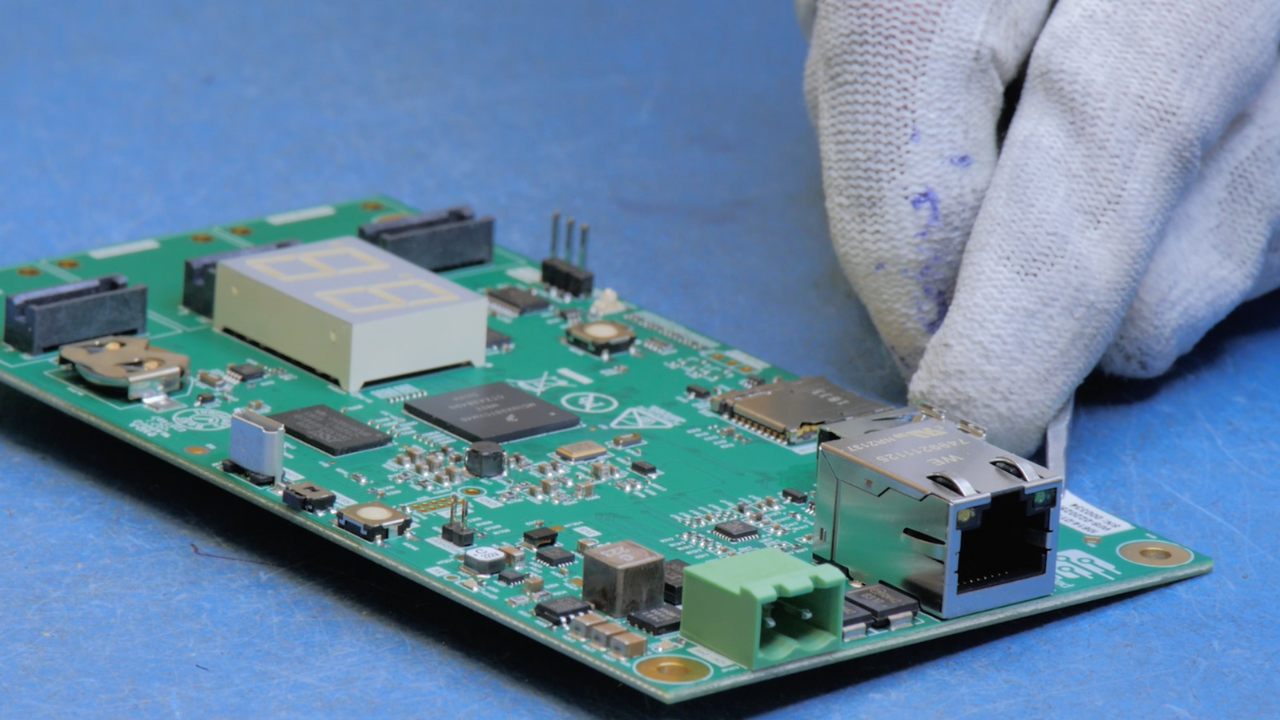
These circuit boards are then built into devices of all shapes and sizes. They might run very simple tasks, or they could do something incredibly complicated. They could be tiny, mounted in a life-saving medical device a patient can wear, or they could be just part of a much larger structure, like an airplane.
Good PCB design and manufacturing gives us:
But this is only possible thanks to over a century of innovation and development.
Tech development never really looks like the movies. As much as we might think that it is a mad scientist slaving away in a lab at all hours of the day and night, developing technology like printed circuit boards happens through labour across many years, shared by many hands. The timeline for PCBs looks a little like this:
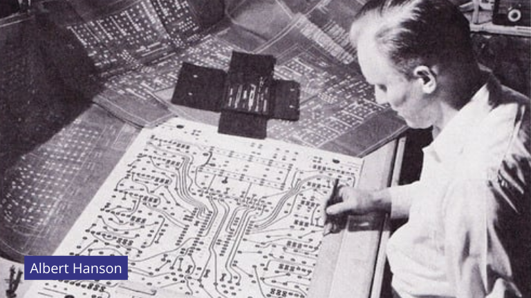
One of the earliest precursors to the modern PCB came about in 1903. A German inventor named Albert Hanson worked on developing the telephone. He filed a patent for flat foil conductors arranged on multilayer boards, allowing for through-hole components mounted on both sides of the board. This is a technique that we still use to this day, right here in our factory at J-TEQ.
The next major development came over 20 years later in 1927, when French inventor Charles Ducas filed his own patent, this one for imprinting wires onto an insulated surface with conductive ink. This created electrical pathways between mounted components, thus allowing us to make the electronic circuits we need and use across the PCB industry and beyond. Ducas's printed wiring concept is one of the first steps in the development of the electroplating used on our modern printed circuit boards.
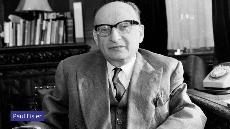
Due to the Great Depression and the stock market crash of 1929, developments in PCB design and manufacture had to slow down a little. The next major leap forward came in the early 1940s thanks to Austrian engineer Paul Eisler. He created what we would recognise now as the first functional PCB.
By adhering a layer of copper foil to his boards, he was able to create conductive pathways for the electronic components he was using. By 1943, he had created radio equipment using PCBs, which were then used in military operations in World War II. PCBs allowed electronic devices to be made smaller and lighter. In addition to their military applications, their commercial promise also began to grow.
Believe it or not, the U.S. Army played a key role in developing mass production methods for PCBs. Through their innovations, making PCBs at a large scale became much easier. Throughout the next few decades, the Cold War led to technological innovation on a grand scale, and this included PCBs. Throughout the 1970s, integrated circuits entered mainstream manufacturing, and with it came a huge surge in demand for PCBs.
This doesn't slow down as we head into the 80s and 90s. Light portable gadgets like Walkmans, cordless and mobile phones, and handheld game consoles all became popular, and every single one needed a PCB in smaller sizes. This is when we also saw the birth of an important procedure in the world of electronics manufacturing—Design for Test (DFT). Following this procedure means that we can design a circuit board in such a way that makes it easy to confirm that the board will work properly, and that we can complete testing quickly and easily, spending less time on troubleshooting and guaranteeing value and quality for customers.
Now into the 21st century, we have seen additional advancements in PCB production and design. As we have advanced etching and soldering techniques, we have been able to create increasingly complex multilayer PCBs to keep up with the incredible advancements in technology we have also witnessed. In addition to this boost in complexity, we have also been able to make boards smaller and smaller, so they take up less and less room.
Just look at your smartphone; the PCB inside needs to be incredibly complex to offer half the functionality of a typical modern phone, and yet the overall device is the size of your hand.
Innovations like surface mount technology, another process we use here at J-TEQ, have helped us to revolutionise the development of PCBs even further. Other technological innovations, like the development of Wi-Fi, 5G, and artificial intelligence, to name just a few, have pushed us forward even further. Even small innovations help us to make more reliable electrical connections, creating stronger and more durable boards that last longer and power many of the devices we take for granted.
We can still see traces of Hanson's original innovation in the PCBs we use today. Just as there have been countless evolutions and forward steps, there is something still worthy about the old practices. Even when assembling electrical circuits and putting boards together, hand-soldering can still be useful for prototyping or small production runs.
Electronics manufacturing has changed massively across even the past 20 years, and yet the basic PCB concept has remained the same. Though the individual components will be very different for the boards going into washing machines, gaming consoles, or telecoms systems, the circuit boards are, on the surface, very similar.
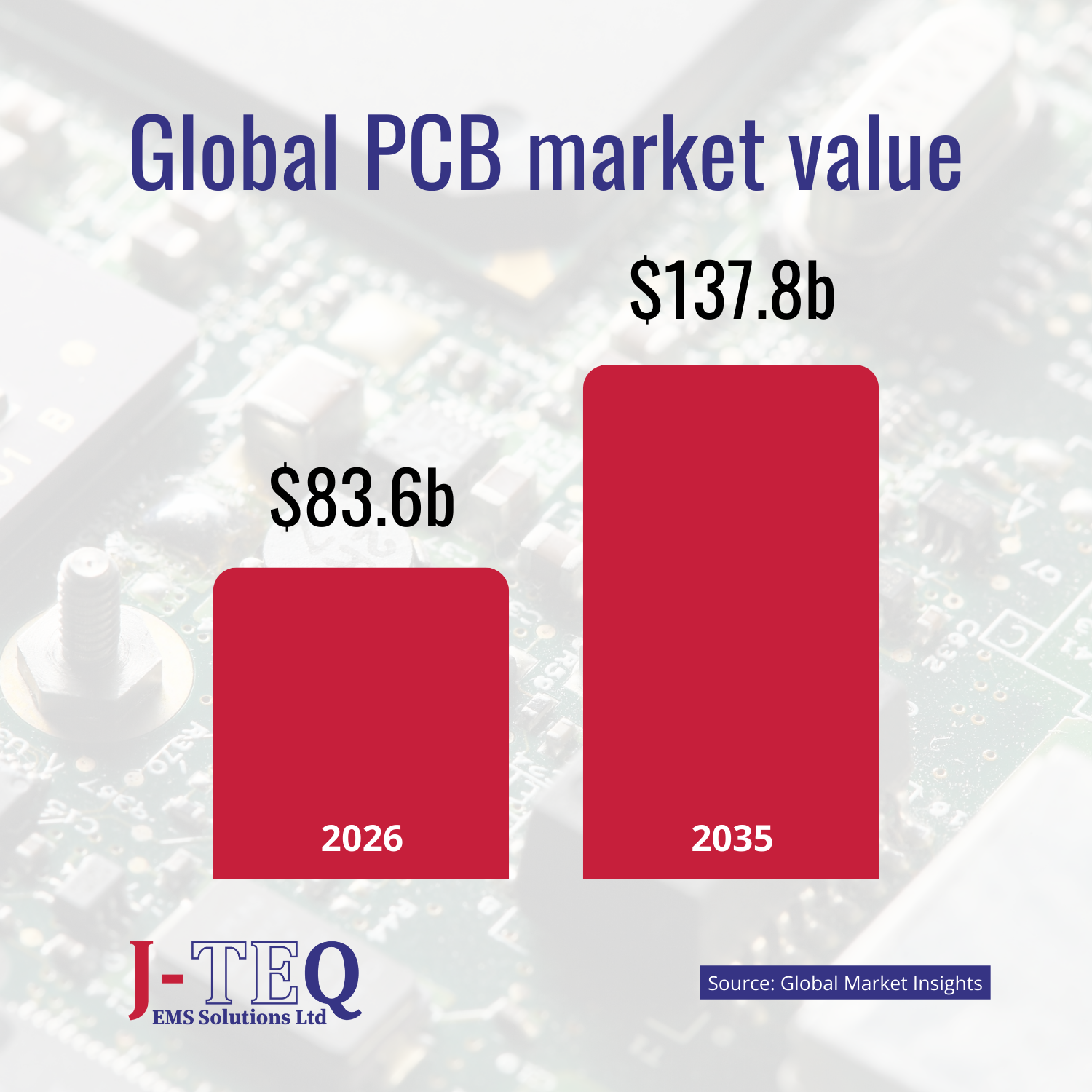
Let's round things out with some useful statistics about PCBs. The market keeps growing and growing, and with devices getting ever more complicated, PCB manufacturers will always need to be ready to keep up.
Looking for an electronic manufacturing service (EMS) partner for your next PCB project? From first prototyping to full-scale manufacturing, J-TEQ can work with you to bring your design to life.
Get in touch with us today to meet all your electronic assembly needs.