Today's devices are smaller, faster, and more powerful than ever before. This ultimately means that the electronic components inside them must also be smaller and more powerful. Surface mount technology (also known by the acronym SMT) is often the method used to pack these crucial components into compact PCBs that power today’s slimline devices.
SMT is one of the main services J-TEQ offers our customers. For many of our customers, it's the optimal solution, and it may be the best choice for your project too. Let's take a closer look at what surface mount technology entails.
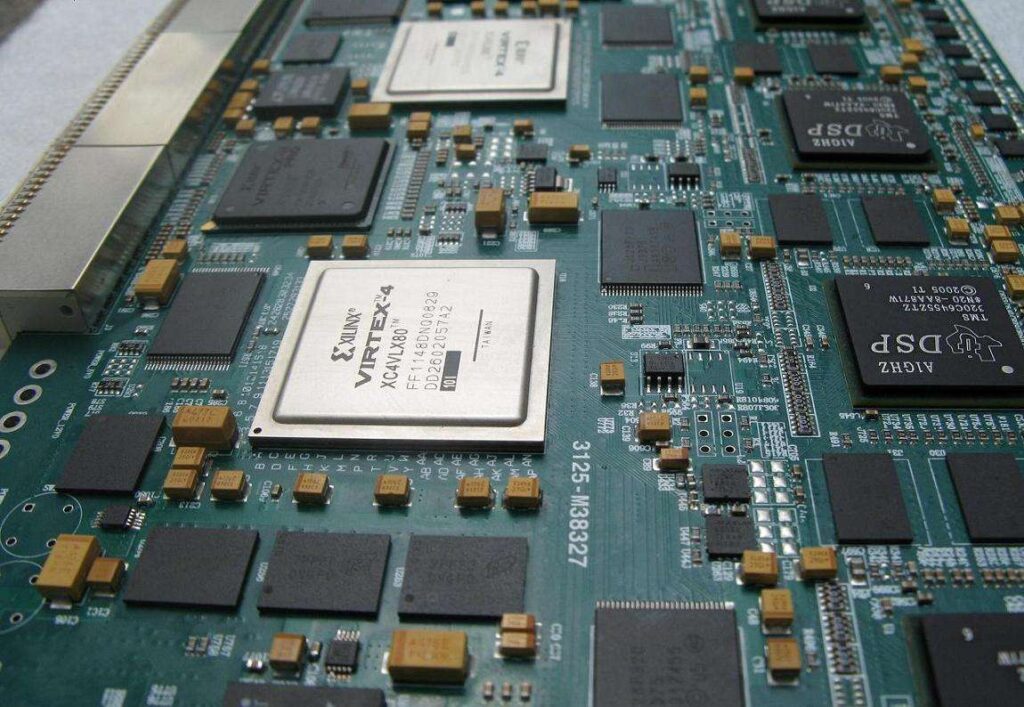
A printed circuit board starts life as just an empty plate. To turn it into the fully functional component that powers your device, we need to fill it with the right components. These components could include resistors, capacitors, transformers, diodes, and many other elements, all of which play a very specific role in how the PCB and the overall device function.
The PCB provides the pathways that allow all components to communicate and function together. SMT is one of the key methods used to connect components on a circuit board. Any components used in the SMT process can be referred to as surface-mount devices, or SMDs.
Choosing SMT assembly methods gives manufacturers a wide range of benefits:
The process used in SMT manufacturing usually follows these steps:
Solder paste is applied to the PCB pads where the components will be mounted. This paste is a mix of tiny solder balls and flux, a chemical cleaning agent used to remove oxides and contaminants from the surface of the board.
The paste is applied over a stencil aligned on the bare circuit board, filling the holes and acting like glue between the board and the components.
An automated pick-and-place machine places the SMDs on the solder-pasted pads. This machine uses vacuum nozzles to pick components from reels or trays and accurately positions them on the PCB to a much higher degree of accuracy and with a greater speed than human eyes and hands. The machine has vision sensors to ensure components are being placed in the correct locations.
Reflow soldering is the process that permanently attaches the components to the board. Once the components have all been placed on the board, it moves through a reflow oven. This equipment has controlled heating zones, allowing the solder to first melt and then create solid joints as it cools.
Inspection and quality control are always important steps for electronic manufacturing services. J-TEQ uses a range of robust quality management systems (QMS) aligned with ISO 9001 and ISO 13485 standards to ensure that all PCBs, whether manufactured using SMT processes or other paths, leave our facilities meeting the highest of standards.
Automated Optical Inspection (AOI) uses cameras to inspect the boards and check for flaws, while x-rays can help identify issues in ball grid arrays and hidden joints.
It is possible to rework and repair some misaligned solders or defects rather than scrap the entire board and create a new one. This may require manual desoldering and repair plus specialist equipment to handle sensitive components.
When the PCBs have been fully quality-checked, they can move on to in-circuit or functional testing. This stage verifies electrical performance and functionality to ensure the PCB will act as it should in its final form. In-circuit testing (ICT) tests individual nets and components, while functional testing powers up the board to test its real-world performance.
If required, cleaning will remove excess contaminants and ensure that the PCBs are in ideal condition. Flux residues can cause issues such as ionic contamination or corrosion if left behind. Cleaning using ultrasonic or solvent-based methods should remove this residue.
Final checks for defects, labelling, and packaging for delivery or integration into higher-level assemblies help to ensure that everything is as it should be before the PCBs go off to their respective customers.
There are situations where SMT may not be the most suitable manufacturing option. The main alternative process used is through-hole assembly. Through-hole assembly is preferred for components that are incompatible with surface mounting, such as large transformers or certain types of semiconductors.
PCBs that will be placed under high levels of thermal or vibrational stress (such as that which occurs in the aerospace and defence sectors, or in the industrial sector) are better assembled using through-hole mounting over SMT.
Through-hole may also be the better option for small product runs, such as a small-batch prototype production, as SMDs are typically smaller and more densely packed than through-hole components. This means there is less surface area for marking part IDs and component values, two useful steps during the prototyping process.
J-TEQ will always advise the best manufacturing process for your needs, so you can be assured that you will receive the highest quality products for your project.
With the capacity for higher component density and mass production through automated manufacturing processes, surface mount technology proves time and time again why it is one of the most popular choices for electronic services manufacturing.
Whether you have a clear idea of how your surface mount components will come together in the final board or you need a full turnkey solution from start to finish of the manufacturing process, J-TEQ is the partner for you. Our experts can help you shorten lead times, simplify logistics, and reduce commercial risk.
Ready to streamline your electronics manufacturing? Get in touch today to discuss your project and how J-TEQ can help you take it from plans to design to reality.