Solder Screen Stencil Design and Solder Reflow Technologies for PCB Assembly
Introduction
In the realm of Printed Circuit Board Assembly (PCBA), solder screen stencils play a pivotal role in ensuring accurate solder paste deposition on Surface Mount Technology (SMT) pads. The precision of stencil design directly impacts the assembly quality, affecting component placement, solder joint integrity, and overall reliability. This report delves into the technical considerations of stencil design, referencing industry practices at J-TEQ EMS Solutions Ltd., alongside insights from our industry leading stencil and soldering technology providers. Additionally, the report evaluates the two primary solder reflow methods—Convection Oven Reflow and Vapor Phase Reflow with vacuum—highlighting their respective merits and integration within advanced PCBA manufacturing processes.

Solder Screen Stencil Design
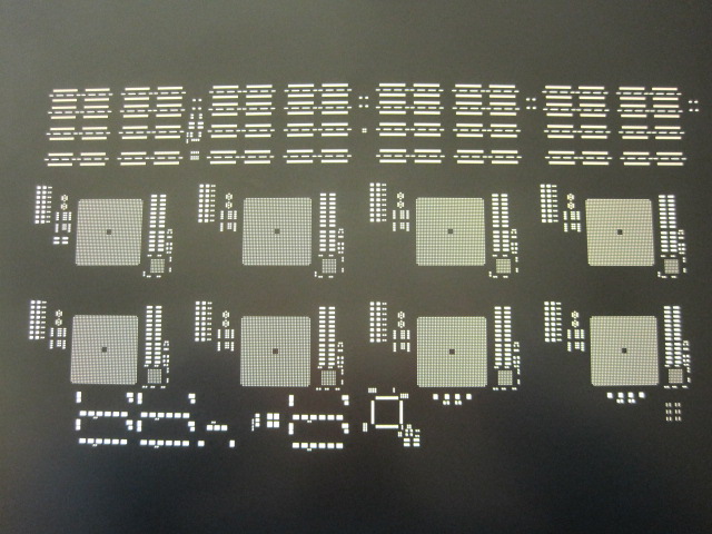
Stencil design is a critical step in the SMT process. The stencil serves as a template to apply solder paste precisely onto the PCB, ensuring correct solder volume for reliable component attachment. At J-TEQ EMS Solutions Ltd., the focus on quality and precision drives the adoption of advanced stencil manufacturing techniques.
Key Considerations in Stencil Design
Aperture Design
The size and shape of the stencil apertures are crucial for controlling the amount of solder paste deposited. Aperture design should account for:
Component type: Smaller components like 0201 or 01005 require precise apertures to avoid excessive solder, which could lead to solder bridging.
Pad size and shape: Oval, rectangular, and trapezoidal apertures are commonly used, depending on the pad geometry.
Stencil Thickness
The thickness of the stencil impacts solder volume. A typical stencil thickness ranges from 100 µm to 150 µm, but J-TEQ EMS Solutions Ltd. employs varying thicknesses depending on the product requirements, optimizing for both fine-pitch components and larger power components.
Surface Finish and Material
High-quality stainless steel is often used for stencils, with laser cutting or electroforming techniques ensuring precise aperture creation. Our stencil manufacturers supply custom stencils to meet these specifications, which include electro-polishing to enhance paste release, and multi-level stencils for complex assemblies.
Nano Coating
To further enhance solder paste release, J-TEQ EMS Solutions Ltd. often uses stencils with nano-coating technology, that reduce solder paste adhesion on stencil surfaces, improving printing consistency and reducing cleaning frequency.
Solder Reflow Technologies
Once solder paste is accurately applied, the next critical step is solder reflow. This process melts the solder paste, creating reliable joints between components and PCB pads. J-TEQ EMS Solutions Ltd. utilizes both Convection Oven Reflow and Vapor Phase Reflow with vacuum, selecting the appropriate method based on the product’s requirements.

Convection Oven Reflow
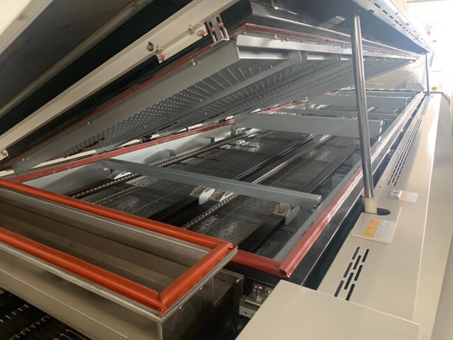
Convection Oven Reflow is the most commonly used soldering method in PCBA. It uses circulating hot air or nitrogen to heat the PCB uniformly, ensuring all components achieve the required reflow temperature.
At J-TEQ EMS Solutions Ltd., convection ovens are extensively used for automotive and aerospace applications, where high throughput and consistent quality are critical. Our solder paste supplier provides technical support for reflow profiling, ensuring optimal thermal performance across diverse product lines.

Vapor Phase Reflow with Vacuum
Vapor Phase Reflow with vacuum technology has gained traction for applications requiring superior solder joint quality and void reduction. This method uses a fluorocarbon liquid, which boils at a precisely controlled temperature, forming a saturated vapor zone. The PCB assembly passes through this zone, ensuring uniform heating. The integration of vacuum technology further reduces voids in solder joints.
J-TEQ EMS Solutions Ltd. leverages Vapor Phase Reflow with vacuum for mission-critical assemblies, such as those in the medical, space and defence sectors, where reliability is paramount. Our stencil suppliers provide precision-engineered stencils that complement vapor phase reflow by ensuring consistent solder paste deposition.
Case Studies and Implementation at J-TEQ EMS Solutions Ltd.
Automotive Electronics
For high-end automotive customers, J-TEQ EMS Solutions Ltd. employs Convection Oven Reflow for large-scale production. The combination of high-quality stencils and precise thermal profiling ensures robust solder joints for in-vehicle electronics, including navigation systems and infotainment units.
Medical Devices
In the medical sector, where reliability and precision are critical, J-TEQ EMS Solutions Ltd. adopts Vapor Phase Reflow with vacuum. For instance, life-support monitoring devices require minimal voids in solder joints to ensure longevity and reliability. Our stencil manufacturer partners advanced stencils, coupled with J-TEQ's reflow expertise, deliver superior results.
Aerospace/Space Applications
Aerospace PCBA demands adherence to stringent quality standards. J-TEQ integrates both convection and vapor phase reflow methods, depending on the application. Navigation aids and sensor systems benefit from the uniform heating of vapor phase reflow, ensuring optimal performance in high-altitude environments.
Conclusion
Solder screen stencil design and reflow technology are critical to the success of PCBA. J-TEQ EMS Solutions Ltd. demonstrates a commitment to excellence by integrating advanced stencil technologies from industry leaders in conjunction with our industry leading solder paste supplier. By leveraging both Convection Oven Reflow and Vapor Phase Reflow with vacuum, J-TEQ ensures superior quality and reliability across diverse industries, from automotive and aerospace to medical and defence. This multi-faceted approach reinforces J-TEQ’s position as a leader in high-quality, reliable electronic manufacturing solutions.